

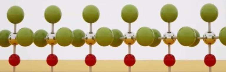
Industrial Atomic Layer Deposition for Image Sensors and Light Sources
September 6, 2019
SEMI spoke with Dr. Mikko Söderlund, sales director for Beneq’s semiconductor business, about trends in Atomic Layer Deposition (ALD) applications. Söderlund shared his views ahead of his presentation at SEMI MEMS & Imaging Sensors Summit, 25-27...
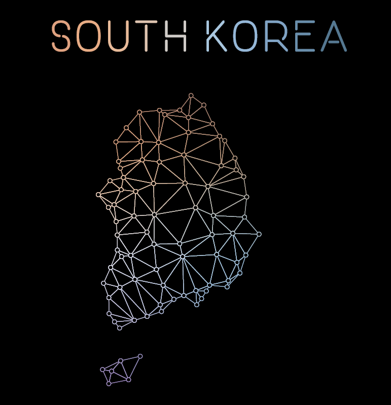
SEMI Korea Members Day: Takeaways and Tech Trends as Korea Leads in Fab Investment
September 28, 2018
Korea is on track to top all other regions in fab investment, spending $63 billion between 2017 and 2020, with powerhouses Samsung Electronics Co. and SK Hynix leading the way, according to latest World Fab Forecast Report by SEMI. Samsung...