

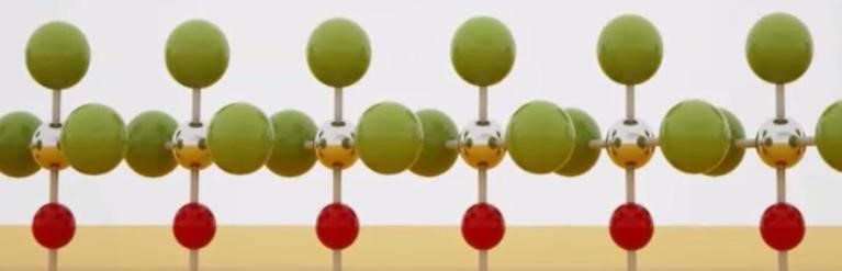
Industrial Atomic Layer Deposition for Image Sensors and Light Sources
SEMI spoke with Dr. Mikko Söderlund, sales director for Beneq’s semiconductor business, about trends in Atomic Layer Deposition (ALD) applications. Söderlund shared his views ahead of his presentation at SEMI MEMS & Imaging Sensors Summit, 25-27...

The Future of MEMS
Despite market saturation and stagnation saddling many business sectors, MEMS remains a shining star in the semiconductor industry. Opportunities in automotive, consumer electronics, mobile, medical are rising. What is supporting this industry...
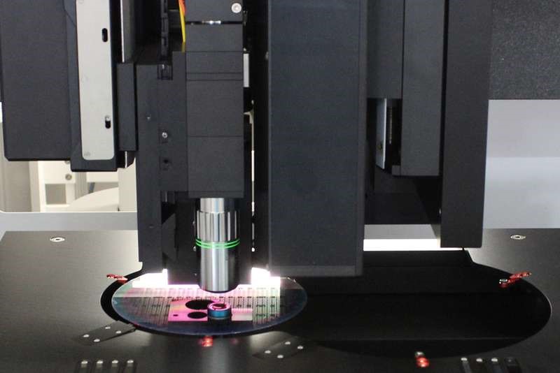
Multi-Sensor Metrology Tools for Hybrid Metrology
SEMI spoke with Thomas Fries, founder and CEO of FRT GmbH, about how hybrid metrology is shaping multi-sensor metrology tools to enhance measurement precision as the industry moves away from a single-sensor approach.
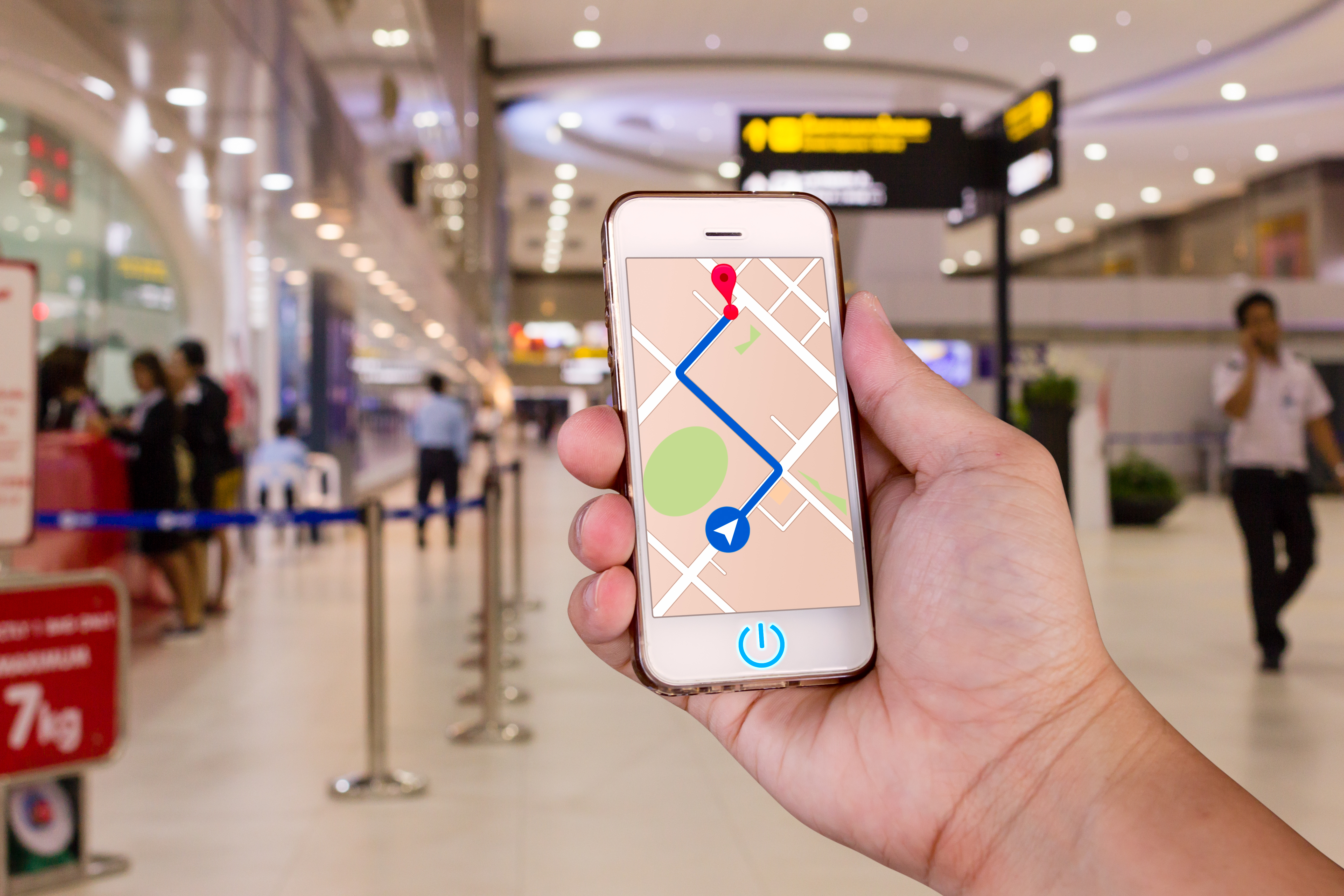
Sensor Fusion: Indoor Localization and Augmented GPS Applications
Tracking and localization technologies typically integrate with Wi-Fi and Bluetooth signals to pinpoint the location of people and objects. But what if a venue can’t install beacons or routers, or afford to deploy Wi-Fi or Bluetooth networks? Thanks...

Making Wearables Always Wearable With MEMS Sensor Technology
Ahead of his presentation on the future of wearables at the European MEMS & Sensors Summit 2018, 19-21 September in Grenoble, France, SEMI spoke with Dr. Peter Weigand, vice president, Business Strategy and Portfolio Management, Bosch Sensortec...